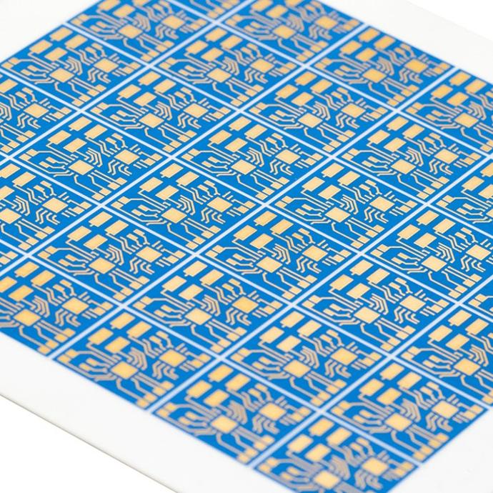
THICK FILM SUBSTRATE MANUFACTURING SERVICES
At CMS Circuits, Inc., we specialize in delivering cutting-edge thick film substrate solutions that empower innovators across Aerospace, Medical, Commercial, and Semiconductor industries. With advanced screen printing and etching technologies, we produce high-precision, multilayer thick film circuits on a variety of substrates, including alumina, aluminum nitride, beryllium oxide, fused silica, and ferrite.
Our capabilities include:
- Precision Manufacturing: Achieving line widths as fine as 0.001” with 0.001” spacing through etched thick film processes, and 0.004” lines with 0.004” spacing via screen printing, ensuring high-density circuitry for compact, reliable designs.
- Versatile Substrate Options: Offering standard and specialty materials like sapphire and ferrite to meet unique application requirements, from optoelectronics to RF needs.
- Multilayer Expertise: Crafting complex, multilayer circuits with ceramic vias, coated or filled with conductive materials, for robust performance in harsh environments.
- Custom Solutions: Engineering tailored thick film substrates, including heaters, thermistors, and sensors, to enable high-reliability products that operate in extreme conditions, from -50°C to 150°C.
- Innovative Applications: Supporting next-generation technologies with printed coils for Bluetooth, NFC, and wireless charging, as well as wearable and implantable device miniaturization.
Certified to ISO13485, ISO9001, and AS9100 standards, we combine mature processes with modern innovation to deliver cost-effective, high-quality solutions that keep you ahead in a competitive world. At CMS Circuits, we don’t just build circuits—we enable the future.
This technology is used in demanding applications where long life, thermal endurance, mechanical strength, thermal conductivity, high density electrical interconnection, low dielectric losses, etc., are needed
Features:
- Through hole connections from front to back of ceramic standard process
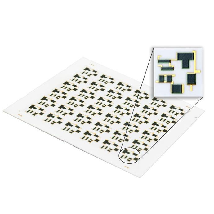
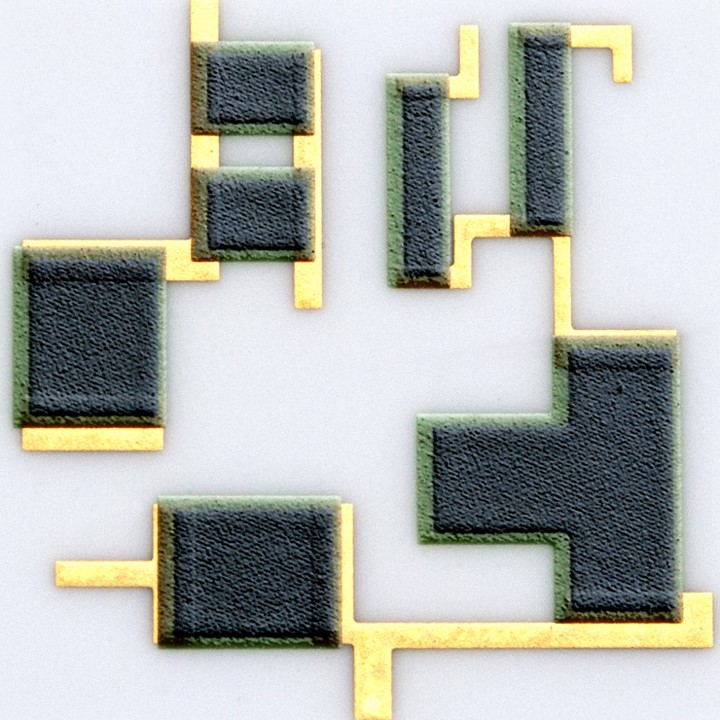
- Screen printed resistors on both front and back is standard process
- Gold conductors can be wire bonded with both gold wire and/or alumina wire
- Solderable metallization is available that can be integrated with gold wire bondable conductors
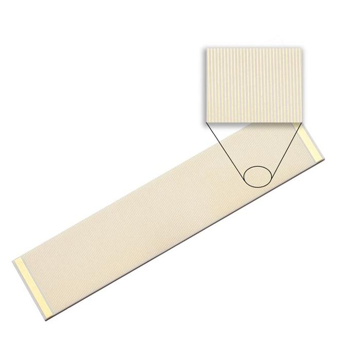
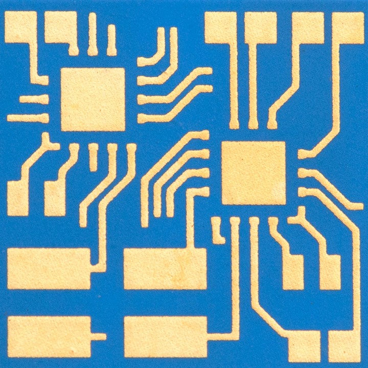
Etched Thick Film
For product with much tighter spacing requirements, etched thick film substrates are the best solution and are more cost effective.
Features:
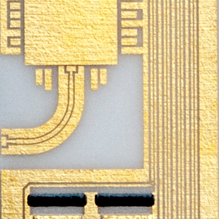
- Etched standard 2 mil (0.002") lines and spaces 1 mil (0.001") lines special request) on gold. Etched Gold Thick Film has better insertion loss at higher frequencies than comparable Thin Film RF circuits
- Lange couplers available that do not require wire bonding to tie coupler elements together
- Gold and Silver etching available
Multilayer Thick Film Screen Printing
These substrates consist of screen printed conductor layers, separated by dielectric layers, which can be interconnected by vias. This allows high density interconnection.
Features:
- Ten layers or more available with our standard process
- 10 mil square vias or larger available with our standard process
- Dielectrics available that will allow intermixing of gold and silver metallization
- Multilayer capability both front and back with through hole interconnections
Heaters
When it comes to turning thick film concepts into reality, CMS Circuits stands out as an industry leader. Renowned for its expertise in thick film technology, CMS Circuits combines cutting-edge manufacturing with a customer-centric approach to deliver unparalleled solutions.
Features:
- Rapid Thermal Response: up to 200°C/sec heating rates
- Uniform Temperature Distribution: ±2% across surfaces
- High Power Density: Up to 100 W/in²
- Operating Range: -50°C to 150°C
- Common Applications:
- Medical Devices: Blood analyzers, surgical tools, and patient warming systems.
- Aerospace: De-icing systems, sensor heating, and cabin climate control.
- Industrial: Process heating, 3D printing beds, and battery thermal management.
- Consumer Electronics: Vape devices, wearable tech, and small appliance heating.
In a market crowded with options, CMS Circuits’ commitment to excellence and adaptability positions it as the premier thick film service manufacturer, ready to elevate your heating solutions beyond what traditional heaters can achieve.
Custom/Specialty Applications
When standard thick film processes aren’t able to work with a design, multiple processes can be incorporated to achieve strict design requirements.
Features:
- Etch layer on top of multilayer
- Etching available on all metal layers of a multilayer structure
- Photo imageable dielectrics available for multilayer structures
- Integrated resistors and capacitors available with etch technology
